Sir Boateng
  • TECH & ELECTRONICS
    • Arduino Projects
    • Proteus
    • Applied Electricity
  • TUTORIALS
    • Blogging
    • Business
  • EDUCATION
    • GES Resources
    • NTC Resources
    • Scholarships
    • Universities & Colleges
  • REVIEWS
    • Comparisons
  • MORE
    • Contact Us
    • Disclosure Statement
    • Disclaimer
    • Privacy Policy
No Result
View All Result
Sir Boateng
No Result
View All Result

250W PWM inverter circuit using SG3524 and BJT

by Sir Boat
24th November 2022
in Electronics
82 1
0
pwm inverter circuit diagram
95
SHARES
296
VIEWS
Share on FacebookShare on TwitterShare on WhatsApp
ADVERTISEMENT

This project depicts a 250W PWM inverter circuit built around the IC SG3524. The SG3524 is an integrated switching regulator circuit that includes all of the circuitry needed to build a single-ended regulator.

Moreover, the SG3524’s internal circuitry includes a pulse width modulator (PWM), oscillator, voltage reference, error amplifier, overload protection circuit, output drivers, and other components.

The SG3524 is at the heart of this PWM inverter circuit, which can compensate for variations in the output load.

A change in output load directly affects the output voltage in a non-PWM inverter (when output load increases, output voltage decreases, and vice versa), but in a PWM inverter, the output voltage remains constant over a range of output load.

The Circuit diagram.

250W PWM inverter circuit diagram

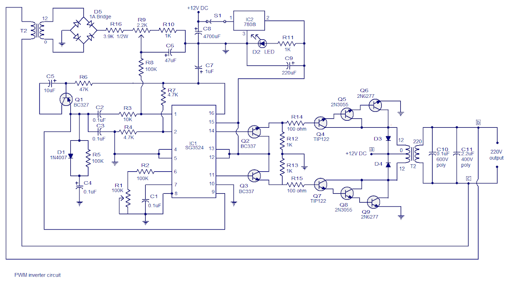
About the 250W PWM inverter circuit.

The frequency of the IC’s internal oscillator is set by resistor R2 and capacitor C1. The oscillator frequency can be fine-tuned using Preset R1.
Pins 14 and 11 are the emitter terminals of the IC’s internal driver transistor.

Also, check these related articles specially selected for you:

  • ESP8266 Development Board Programming with Arduino IDE
  • Transistors: The grandmaster in Modern Electronics
  • Circuit Breaker (Principles and Operation)
  • New GES Curriculum for Basic Schools
  • How to install all TM1 Laptop drivers

The driver transistor collector terminals (pins 13 and 12) are linked together and connected to the +8V rail (output of the 7808). Pin 14 and 15 of the IC provide two 50Hz pulse trains that are 180 degrees out of phase.

To produce 250W these are the PMW signals that drive the inverter’s transistor stages as follows. When the signal at pin 14 is high, transistor Q2 turns on, causing transistors Q4, Q5, and Q6 to turn on. Current flows from the +12V source (battery) connected at point a (marked with label a) through the upper half of the transformer (T1) primary and sinks to the ground via transistors Q4, Q5, and Q6.

SEE ALSO:  Top 8 Arduino Projects in Proteus with Source Code

This FM transmitter project also uses only transistors and works very great.

As a result of the electromagnetic induction, a voltage is induced in the transformer secondary, and this voltage contributes to the upper half cycle of the 220V output waveform.

During this time, pin 11 will be low, and the subsequent stages will be inactive. When IC pin 11 goes high, Q3 is turned on, and as a result, Q7, Q8, and Q9 are also turned on.

This 250W PWM inverter circuit causes current flows from the +12V source (labelled a) through the lower half of the transformer primary and sinks to the ground via transistors Q7, Q8, and Q9, and the induced voltage at the T2 secondary contributes to the lower half cycle of the 220V output waveform.

The inverter circuit’s output voltage regulation section operates as follows. The inverter output (T2 output) is tapped from points b and c and supplied to the transformer T2’s primary to obtain 250W. This emulates the PWM inverter circuit functionality.

ADVERTISEMENT

This high voltage is stepped down by transformer T2, rectified by bridge D5, and this voltage (proportional to the inverter’s output voltage) is supplied to pin1 (inverting input of the IC’s internal error amplifier) via R8, R9, R16, and this voltage is compared with the internal reference voltage.

This error voltage is proportional to the deviation of the output voltage from the desired value, and the IC adjusts the duty cycle of the drive signals (at pins 14 and 12) to restore the desired output voltage.

Preset R9 can be used to adjust the inverter output voltage because it directly controls the amount of voltage fed back to the error amplifier section from the inverter output.

SEE ALSO:  Innovative Project Ideas for Engineering Students

For powering the IC and its associated circuitries, IC2 and its associated components generate an 8V supply from the 12V source. Diodes D3 and D4 are freewheeling diodes that protect the driver stage transistors from voltage spikes caused by switching the transformer (T2) primaries.

In this 250W PWM inverter circuit, R14 and R15, respectively, limit the base current of Q4 and Q7. R12 and R13 are pulldown resistors for Q4 and Q7, preventing them from accidentally turning on. C10 and C11 are used to eliminate noise from the inverter output. C8 is a voltage regulator IC 7808 filter capacitor. R11 controls the current flowing through the indicator LED D2.

Notes.

  • To get the best result from this 250W PWM inverter circuit, place the SG3524 in a holder or IC socket.
  • Except for C10 and C11, all capacitors must be rated at least 15V.
  • The inverter’s output voltage can be adjusted using Preset R9.
  • Preset R1 can be used to change the operating frequency of the inverter.
  • Heatsinks are required for transistors in the driver stage.
  • T2 is a 1A transformer with a 220V primary and a 12V secondary.
  • T1 is a 300VA transformer with a primary voltage of 12-0-12 V and a secondary voltage of 220V.
  • Mica sheets must be used to isolate driver transistors from the heatsink.
    These transistors’ mounting kits are widely available on the market.
  • The 7808 can be equipped with an optional finned aluminium heatsink.
  • If a 1A bridge is not available to build this 250W PWM inverter circuit, construct one with four 1N4007 diodes.
Join Our Tech & Edu Forum
Tags: electronics circuitinverter circuitpwm inverter
ADVERTISEMENT
Previous Post

Getting Started with LoRa RYLR998 and Arduino

Next Post

Arduino vs Raspberry Pi: Which one is good for your project?

Sir Boat

Sir Boat

Boateng Oduro is passionate about learning new technologies and working on them. He is a teacher and an engineer who loves to read, write, and teach. He's always curious about things and very determined to track the latest technologies and the trends for the future.

Leave a Reply Cancel reply

Your email address will not be published. Required fields are marked *

Recent Posts

A photo of the Best Universities in Ghana for International Students

The Best Universities in Ghana for International Students

22nd May 2023
A photo showing the heads on comparison between grammarly free and premium

Grammarly free vs premium – which one is good?

22nd May 2023
A picture showing the Comprehensive Guide to the New Basic and JHS Curriculum

A Comprehensive Guide to the New JHS Curriculum

16th May 2023
A picture comparing Grammarly and Quillbot and explaining Which AI Writing Tool is the Best for You

Grammarly vs Quillbot: Which AI Writing Tool is the Best for You?

22nd May 2023
A picture showing How to Secure Fully Funded Scholarships for Canada in 2023

How to Secure Fully Funded Scholarships in Canada in 2023

22nd May 2023
An image showing the Top 10 Best Website Hosting Providers in 2023 to choose from.

Top 10 Hosting Providers in 2023 – Find the Best One for Your Website

17th April 2023

Categories

  • Applied Electricity & Electronics (4)
  • Arduino Projects (8)
  • Blogging (5)
  • Business (4)
  • Comparisons (3)
  • Education (28)
  • Electronics (21)
  • GES Resources (12)
  • NTC Resources (3)
  • Product and Service Reviews (6)
  • Proteus (2)
  • Scholarships (2)
  • Tutorials (22)
  • Universities & Colleges (1)

Sir Boateng Online is a platform for technology and electronic projects, tutorials and educational resources. Aside creating Tech tutorials, we also provide Education, GES and NTC resources such as teaching syllabus, lesson notes, scheme of work, GES promotion and NTC trial questions. We help people to create website for blogging, business and organizations such as school, church, club etc.

Popular Categories

Applied Electricity & Electronics Arduino Projects Blogging Business Comparisons Education Electronics GES Resources NTC Resources Product and Service Reviews Proteus Scholarships Tutorials Universities & Colleges

Stay Connected

  • About Me (Sir Boateng Oduro)
  • Forum
  • Disclaimer
  • Privacy Policy
  • Terms and Conditions

© 2023 Sir Boateng Online - Developed by Lizbotech.

No Result
View All Result
  • TECH & ELECTRONICS
    • Arduino Projects
    • Proteus
    • Applied Electricity
  • TUTORIALS
    • Blogging
    • Business
  • EDUCATION
    • GES Resources
    • NTC Resources
    • Scholarships
    • Universities & Colleges
  • REVIEWS
    • Comparisons
  • MORE
    • Contact Us
    • Disclosure Statement
    • Disclaimer
    • Privacy Policy

© 2023 Sir Boateng Online - Developed by Lizbotech.

Welcome Back!

Login to your account below

Forgotten Password?

Retrieve your password

Please enter your username or email address to reset your password.

Log In
This website uses cookies. By continuing to use this website you are giving consent to cookies being used. Visit our Privacy and Cookie Policy to read more.